| Core Information | Detailed Content |
| Customer Introduction | An automotive parts supplier, one of the technology giants in the global automotive industry |
| Chip Types | UFS chips, NORFLASH chips, MCU chips, SoC chips |
| Core Challenges | Special chip demand: UFS large-capacity storage chips
This solution is mainly adapted for KIOXIA UFS 3.1 chips (formerly Toshiba Storage), designed specifically for high-performance mobile/industrial/automotive scenarios: |
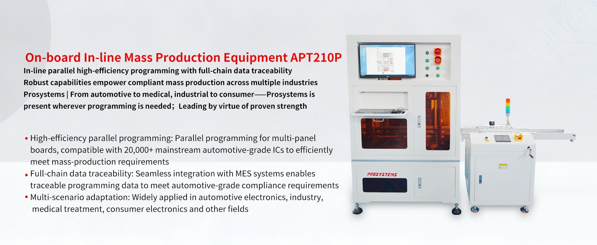
| Automated production line integration: SN serial number automatically obtained; after programming, laser marking/spray coding automatically triggered to realize product unique identifier flow |
| Real-time MES data interaction: uploading SN, programming results, operation time and other parameters in real time to make the production process transparent |
| Full-lifecycle traceability: building complete product archives based on MES, tracing from finished products to raw materials and production processes to ensure quality compliance |
| Customized Solution | The solution adopts a three-tier architecture of 'offline end + in-line end + data layer', each performing its own duties and coordinating to create a fully automatic, highly precise and traceable chip programming solution |
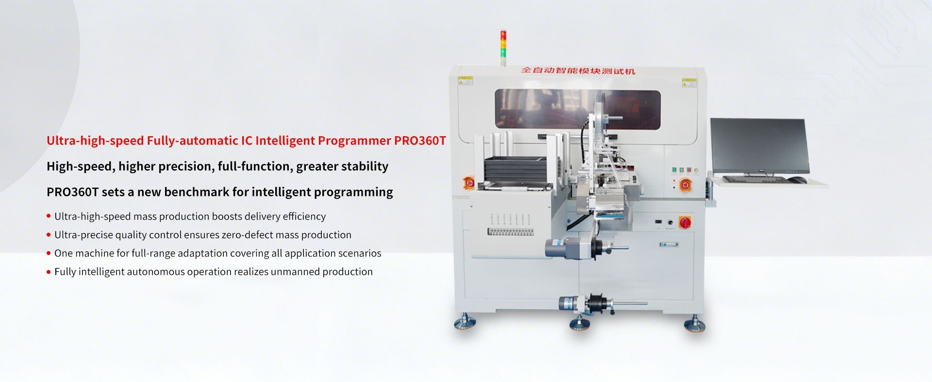
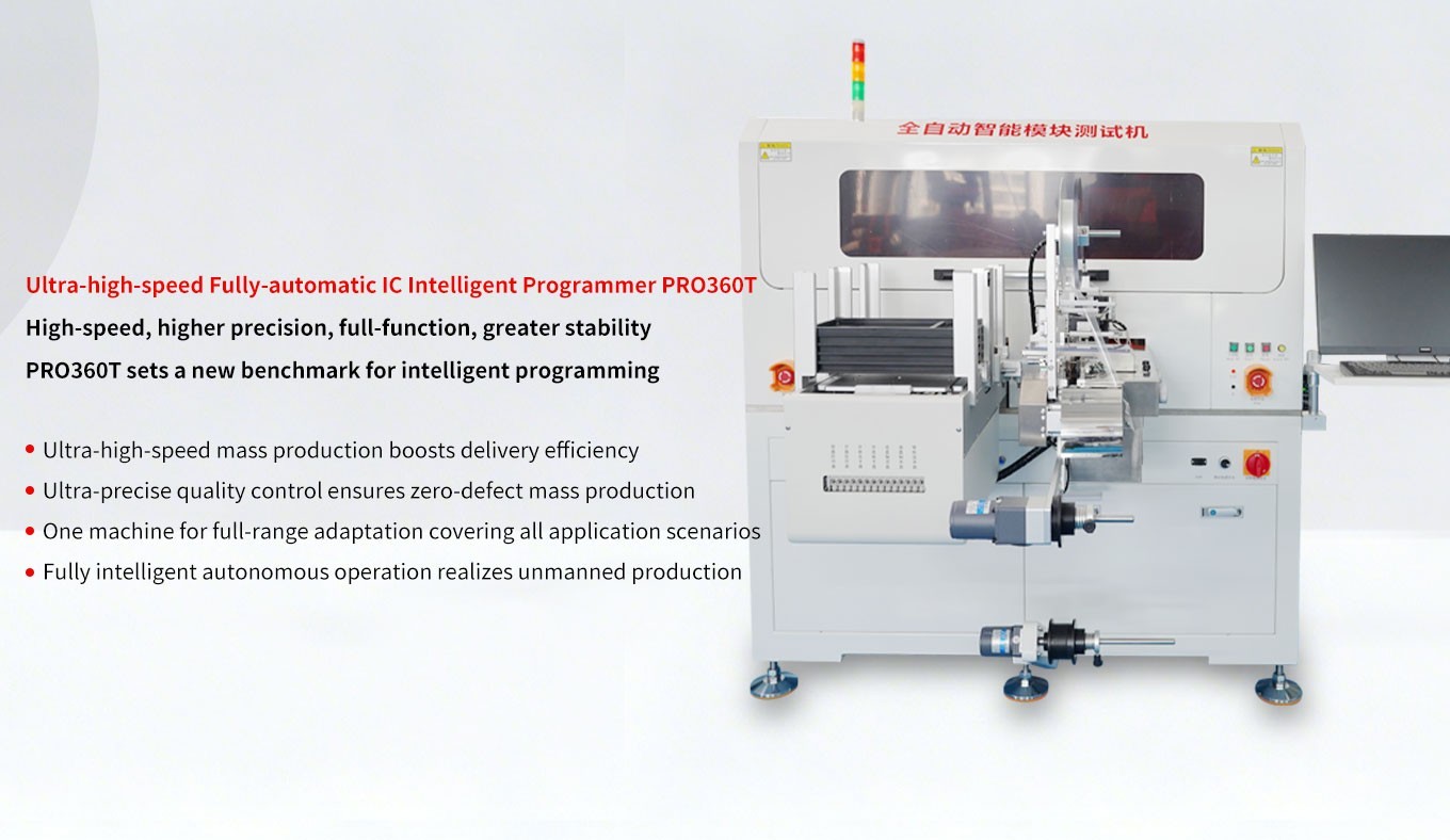
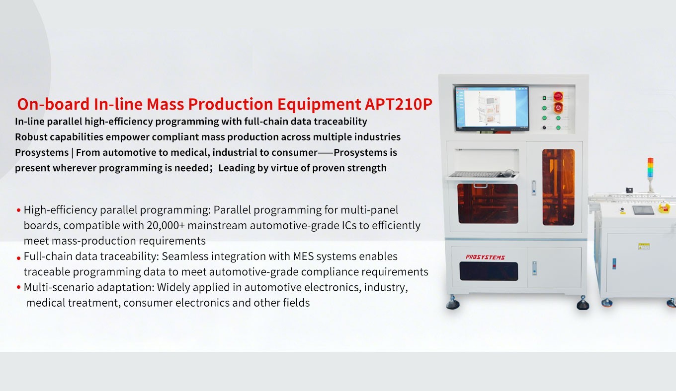
| Core architecture: offline end (PRO360T+ALL300GU2/G2) → in-line end (SMH FlashRunner 2.0 (NXG)) → data layer (MES system) |
| Core process: circuit board online → MES issues SN → PRO360T offline programming + laser marking → data upload to MES → transfer to in-line station → SMH FR 2.0 (NXG) programming → data upload to MES → full-process verification → qualified outflow |
| Project Results | 1. UFS offline programming technology innovation, capacity increased several times.
CT efficiency several times better than in-line programming, precisely breaking through the large-capacity UFS programming capacity bottleneck, achieving doubled output per unit time and solving the customer's core production pain point. |
2. Hybrid process innovation, multi-process integrated.
Innovatively integrating offline + in-line programming processes, integrating laser, marking and programming all in one process to create an automated special production solution. Multi-process seamless connection reduces manual intervention and improves production efficiency and product quality consistency. |
3. High-level encryption security, protecting core technology.
Supports real-time linkage between SN programming dynamic data and customer SBS system, achieving unique binding of chip data. |
4. Full-process data traceability, ensuring quality compliance.
MES system intervenes throughout the entire chain, from SN issuance, programming process, identifier upload to final verification. Every chip's data is searchable, controllable and traceable, building a full-lifecycle quality archive and meeting industry quality compliance requirements. |
| Application Scenarios | Intelligent driving, Advanced Driver Assistance Systems (ADAS), mobile phone/tablet consumer electronics products, etc. |

 EN